
Characterise Semiconductor Materials with Nanoscale IR
How nanoscale IR spectroscopy (AFM-IR) can be used for nanoscale chemical analysis of semiconductor materials in semiconductor device development, manufacturing, process control and failure analysis. Identify chemical components, organic contaminants and analyse defects.
Blue Scientific is the official Nordic distributor for Bruker Anasys in Norway, Sweden, Denmark, Finland, Iceland). For more information or quotes, please get in touch.
Bruker Anasys nanoIR3
Contact us on +44 (0)1223 422 269 or info@blue-scientific.com
Follow @blue_scientificLimitations of Traditional Techniques
A variety of techniques are used for identifying chemical components on semiconductor materials at the submicron and nanoscale:
- SEM/EDX (Scanning Electron Microscopy with Energy Dispersive X-ray spectroscopy) is the industry standard surface analysis technique, delivering nanometre-scale resolution and semi-quantitative elemental analysis. While useful for information about surface defects and contamination, it’s limited with regards to organic materials.
- Infrared (IR) spectroscopy chemically characterises organic species that can’t be identified with SEM/EDX. However, traditional IR techniques are limited by Abbe diffraction laws to resolutions of 3–10 µm.
- AFM (Atomic Force Microscopy) provides high resolution topographic maps of the surface. However until now, AFM could not chemically characterise materials underneath the tip.
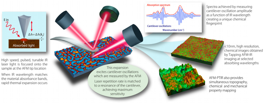
Nanoscale IR Spectroscopy
Nanoscale IR spectroscopy overcomes these limitations by combining AFM and IR, for nanoscale FTIR spectroscopy using photothermal IR spectroscopy (PTIR). This gives you:
- Precise chemical identification of IR spectroscopy
- Nanoscale capabilities of AFM
You can chemically identify materials at a spatial resolution <10 nm and with monolayer sensitivity, breaking the diffraction limit by >100x. AFM-PTIR spectra measure sample absorption, and are not affected by the optical properties of the tip or sample, so they correlate well with conventional bulk IR spectra.
Bruker Anasys nanoIR3
The nanoIR3 is a nanoscale infrared spectrometer for chemical imaging and property mapping, with full-featured AFM.
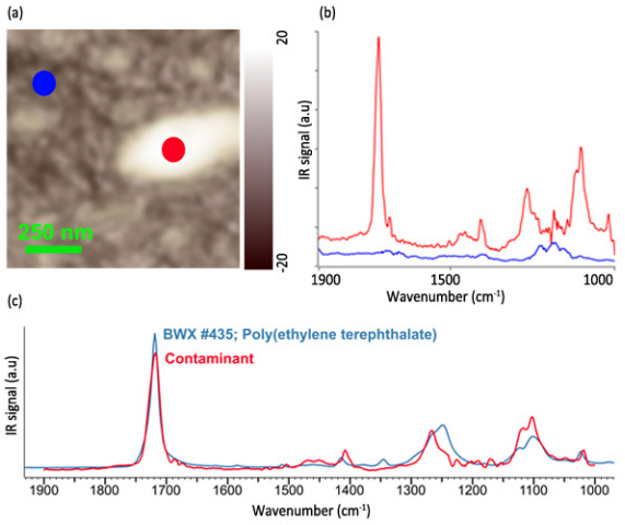
Identify Organic Contaminants
In this example, contaminated silicon wafers were chemically characterised at the nanoscale, using the nanoIR3. The contaminants were located using high resolution AFM, then measured with nanoIR.
The AFM height image indicated a variation in thickness in the contaminant residue of 20-100 nm, from human skin tissue. A point of interest was identified and the laser wavelength was scanned to acquire the nanoIR spectra. Bruker Anasys’ FASTspectra technology accelerated the acquisition time, collecting spectra over the full IR tuning range.
The contamination residue (~30 nm deep) was identified as polyethylene terephthalate (PET), a polymer used in polyester fabrics.
Full details are available in an application note from Bruker.
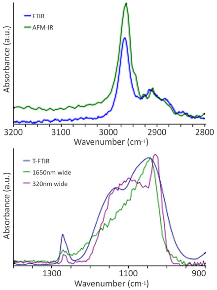
Analysing Defects
Nanoscale IR can also be used to examine defects that occur during manufacturing. This example looks at low-k α-SiOC:H/Cu interconnects, which are particularly sensitive to chemical modifications, sometimes causing defects during the fabrication process. The average width of the material is 1650 nm – 330 nm, which is below the spatial resolution limits of conventional IR spectroscopy.
First an AFM topography image was taken, then nanoIR spectra were acquired from various points on the interconnect. Significant chemical differences were observed for narrow low-k regions compared to thick regions. These differences were observed in both the Si-O-Si and CH stretching areas.
The measurements indicated a loss of terminal methyl (CH3) groups, which can occur during the plasma etching, ashing and CMP steps used to produce inlaid Cu wiring. This results in new chemical bonds and a composition similar to SiO2, as observed in the sample.
Conventional IR spectroscopy would not be able to uncover these defects due to its limited spatial resolution.
Full details of the measurement and results are available in an application note from Bruker.
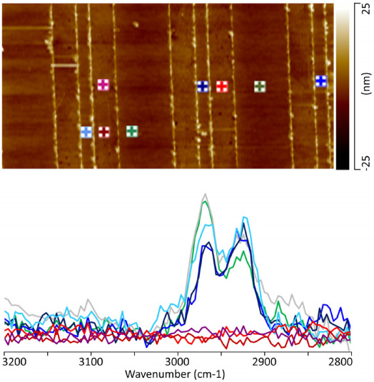
α-SiOC:H/Cu interconnect.
Characterising Semiconductor Structures
The fabrication of ever smaller devices with nanometre-scale domains is a challenge in semiconductor technology. Directed self assembly (DSA) of block copolymers (BCPs) is used for next-generation lithography, providing sub-14 nm nanostructures with controlled placement. Nanoscale pattern fabrication using DSAs with 10-20 nm pitch requires accurate characterisation of size, location and alignment, as well as high resolution material identification.
Recent advances such as Tapping AFM-IR can now deliver a spatial resolution limit below 10 nm. This is ideal for characterising DSA components and defects in failure analysis.
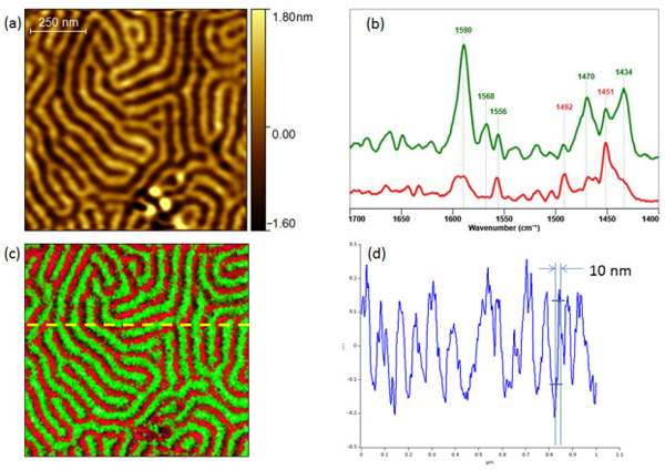
In this example, Tapping AFM-IR was used to measure various block copolymers for manufacturing directed self-assemblies on Si wafers.
The image below shows the AFM topography and nanoscale chemical analysis of polystyrene-poly(2-Vinyl Pyridine) block copolymer [PS-P2VP]. The topography image shows 3-4 nm tall lamellar features with 50 nm pitch. Chemical analysis with Tapping AFM-IR was used to study the chemical composition of the nanopattern.
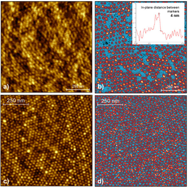
Further measurements were taken on DSAs with various nano-patterns and functional molecules. The results below show chemical maps of spherical DSAs consisting of both PS-b-PMMA and PS-b-P4VP [polystyrene-poly4-vinylpyridine block copolymer]. The measurements delivered excellent chemical specificity and a high spatial resolution of ~4 nm.
Full details of the experiment are available in an application note from Bruker.
More Information
Blue Scientific is the official distributor of Bruker Anasys nanoIR systems. If you’d like any more information about how they can be used for defect and contaminant analysis and characterising semiconductors, please get in touch: