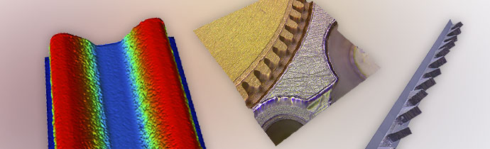
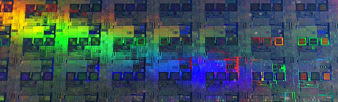
Map defect distribution and variations for process development of materials for electronic / optoelectronic devices. CL is ideal for materials not suitable for photoluminescence spectroscopy.
Self-focusing SIMS is a new technique for measuring the composition of semiconductors and SiGE devices. It’s ten times faster than studying nanometre-scale features directly with methods such as TEM or APT.
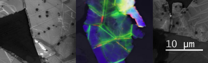
How Raman spectroscopy can be used to characterise semiconductor materials. Measure defects in SiC, crystal quality, stress/strain, homogeneity and more.
Unambiguously identify organic contamination on silicon wafers and micro-electronics with a AFM-IR technique, using the Bruker Anasys nanoIR3.
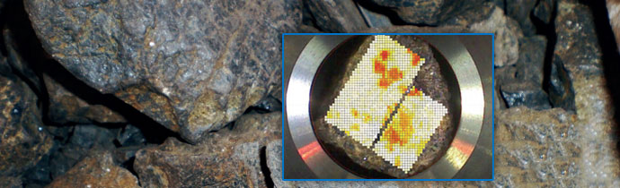
How to analyse elemental distribution in rocks with XRF. In this case study we look at columbite-tantalite (coltan) in rocks from Canada, with the Bruker S8 TIGER Series 2 WDXRF spectrometer. Blue Scientific is the official distributor for Bruker XRF in the Nordic region (Norway, Sweden, Denmark, Finland, Iceland). For more information or quotes, please get in […]