Find out all about CL with Gatan’s new website for users and for those new to the technique.
Download a free copy of Gatan’s electron microscopy software if you’re working from home during COVID-19.
4D STEM is an electron microscopy technique that captures a full 2D diffraction pattern at each pixel position on a STEM map. Access a wealth of diffraction data with your TEM.
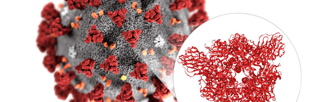
Cryo-EM has been used to generate the first 3D atomic-scale map of the coronavirus (2019-nCoV). This is a key step towards developing a vaccine and treatments for the infection.
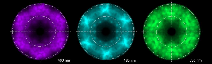
How cathodoluminescence can be used to study the emission patterns of nitride semiconductor micropillars for microLEDs in displays, including wearable devices.
How to use low dose TEM to study beam-sensitive materials with reduced damage, using new electron counting camera technology.
Prepare high quality samples for SEM, EDS, EBSD, cathodoluminescence, EBIC and more with the Gatan PECS II broad argon beam system.
Join us for a demo of the Gatan PECS II (Precision Coating & Etching System) in Sweden on 6-10 May 2019. Sample preparation for SEM, SPM & optical microscopy.
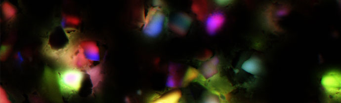
Cathodoluminescence (CL) is a technique for characterising composition, optical and electronic properties with data that correlates with morphology, micro-structure, composition and chemistry at the nanoscale.