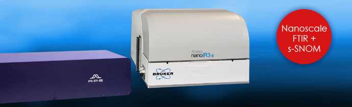
The Bruker nanoIR3-s Broadband is the most advanced s-SNOM based nanoscale FTIR spectroscopy system available, with the broadest spectral range, high resolution nanochemical and nano-optical imaging capabilities.
Join us for a two day conference in Copenhagen about AFM and nanoscale IR spectroscopy (AFM-IR, s-SNOM and O-PTIR).
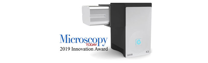
How to use low dose TEM to study beam-sensitive materials with reduced damage, using new electron counting camera technology.
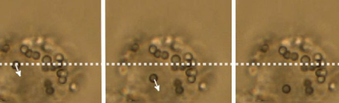
How to use Optical Tweezers to manipulate and measure forces on particles and live cells with the Bruker JPK NanoTracker 2, including adhesion, intracellular studies and cell mechanics.

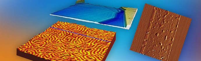
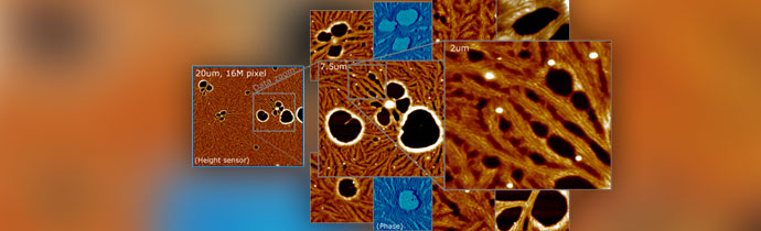
Achieve the highest lateral and vertical resolution with AcuityXR technology on Bruker’s Contour 3D optical microscopes. Break the optical diffraction limit, without compromising the other benefits of white light interferometry. For a limited time, we currently have a trade-in offer to help you benefit from the latest 3D optical microscope technology. Trade in your surface […]
How Bruker have accelerated AFM without compromising image quality – with examples of screening, dynamics and surveying an overview of your sample.
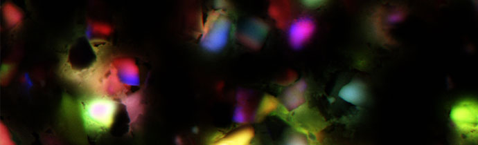
Cathodoluminescence (CL) is a technique for characterising composition, optical and electronic properties with data that correlates with morphology, micro-structure, composition and chemistry at the nanoscale.
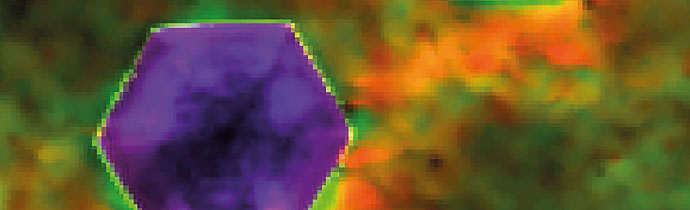
Join Gatan for a webinar introducing cathodoluminescence imaging (CL) – the first of a series about the technique.