+44 (0)1223 422 269 Contact

Posts Tagged ‘sem’

Automated Cross-Sections with the Gatan PECS II

Automated Cross-Sections, Polishing and Delayering for SEM / Optical Microscopy

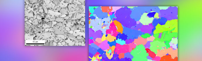
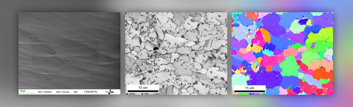
Prepare high quality samples for SEM, EDS, EBSD, cathodoluminescence, EBIC and more with the Gatan PECS II broad argon beam system.

Gatan PECS ii Demo

Gatan PECS II Demonstrations in Sweden

Join us for a demo of the Gatan PECS II (Precision Coating & Etching System) in Sweden on 6-10 May 2019. Sample preparation for SEM, SPM & optical microscopy.

Cathodoluminescence Image

What is Cathodoluminescence? Plus how to add it to your SEM/TEM/STEM

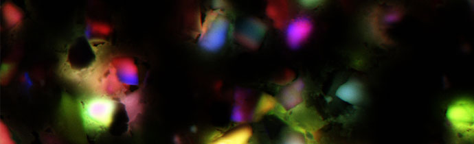
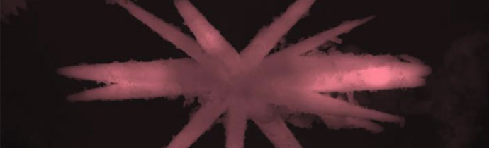
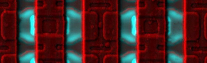
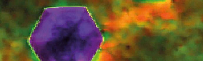
Cathodoluminescence (CL) is a technique for characterising composition, optical and electronic properties with data that correlates with morphology, micro-structure, composition and chemistry at the nanoscale.

Intro to Cathodoluminescence

Cathodoluminescence Webinar: An Introduction

Join Gatan for a webinar introducing cathodoluminescence imaging (CL) – the first of a series about the technique.

Natural History Museum

SEMT Meeting 2018 – London, 12 December 2018

Visit us at the annual SEMT electron microscopy meeting in London on 12th December 2018.

MMC 2019

MMC 2019 – Microscience Microscopy Congress, Manchester, 1-4 July 2019

Visit us at MMC 2019 Microscience Microscopy Congress on 1-4 July 2019 at Manchester Central.

Electron Counting Camera for TEM

Gatan K3 IS: World’s First Counting, Large Format TEM Camera for In-Situ Microscopy

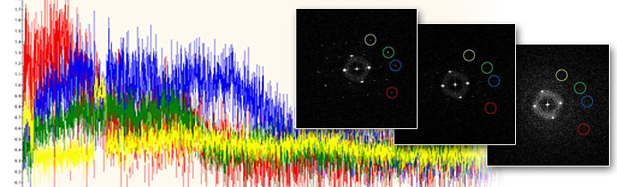
Capture fast in-situ events and reactions at high resolution with the new Gatan K3 IS electron counting, direct detection TEM camera.

In-situ Nanomechanical Testing

In-Situ Nanomechanical Testing Modes for SEM / TEM

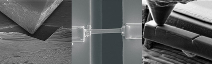
Round-up of in-situ nanomechanical testing modes for SEM and TEM microscopes, including compression, tensile, bend, electrical characterisation, heating and more.

Wavelength-filtered cathodoluminescence

Gatan Monarc: Cathodoluminescence System for SEM

The new Gatan Monarc sets new standards for what’s possible with an SEM-based CL detector.

EBIC (Electron-Beam Induced Current)

What is EBIC? (Electron-Beam Induced Current)

EBIC (Electron-Beam Induced Current) is a technique for characterising the electrical properties of semiconductor materials & devices. Reveal the subsurface electronic structure and analyse defects.