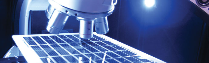
How Raman spectroscopy is used in the development of photovoltaics and solar cells.
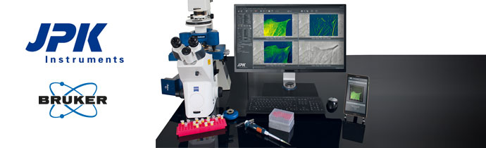
New series of SPM microscopes from Bruker – with models for nanomechanics, electrical AFM and nanoelectrochemistry.

New AFM-nDMA AFM mode from Bruker for quantitative, nanoscale, viscoelastic measurements – for the first time.

Multi-element analysis for refineries and oil manufacturers. Less expensive than WDXRF, with the same analytical performance.
An overview of the range of biological microscopy systems from JPK Instruments, now part of Bruker Nano Surfaces.
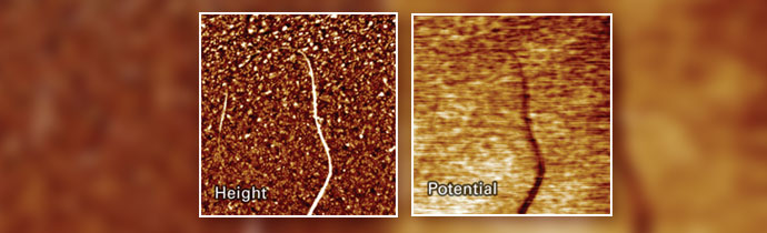
How Bruker’s PeakForce KPFM mode overcomes the common limitations of KPFM (Kelvin Probe Force Microscopy – also known as surface potential microscopy).
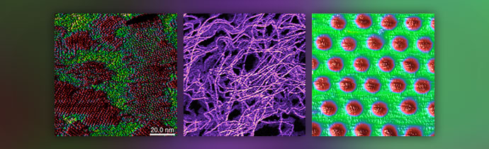
How to map current and conductivity at the nanoscale on fragile samples with AFM, without damaging them or contaminating the probe tip. Useful for lithium battery research, organic photovoltaics and carbon nanotubes.
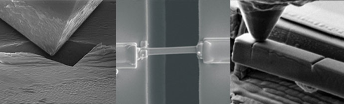
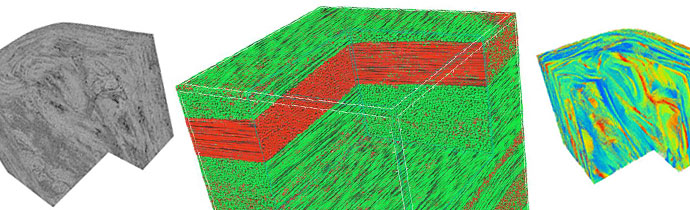
Round-up of in-situ nanomechanical testing modes for SEM and TEM microscopes, including compression, tensile, bend, electrical characterisation, heating and more.
Visit us at the annual Nanoscience Days conference in Finland. Talks, poster sessions, exhibition and networking for researchers in the diverse fields of nanoscience and nanotechnology.