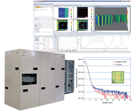
CAMECA IMS Wf & SC Ultra
Low energy SIMS for advanced semiconductor applications
The CAMECA IMS Wf and SC Ultra are designed specifically for dynamic SIMS measurements in the semiconductor industry.
- Wide range of impact energies (100 eV to 10 keV).
- No compromise on mass resolution or primary beam density.
- Unmatched analytical performance.
- High throughput.
The IMS Wf and SC Ultra are equipped for the most challenging semiconductor applications:
- Extra shallow & high energy implants
- Ultra-thin nitride oxides,
- High-k metal gates
- SiGe doped layers
- Si:C:P structures
- PV & LED devices
- Graphene
- …and more
Contact us for more information and quotes:
+44 (0)1223 422 269 or info@blue-scientific.com
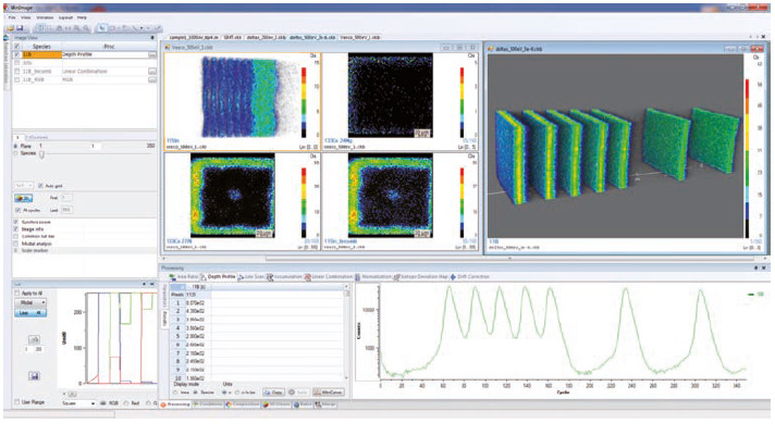
Depth Profiling: Standard to Ultra-Shallow
Advanced semiconductor analysis requires SIMS optimised both for ultra-shallow depth profiling and standard depth profiling applications.
CAMECA’s unique SIMS technology is capable of sputtering samples with a large range of impact energies, from high energy (keV range) for thick structures to Ultra-Low Energy (≤ 150eV) for ultra-thin structures. This flexibility is available for various sputtering conditions, including species, incidence angle, etc.
The CAMECA IMS Wf and SC Ultra are the only SIMS instruments offering these EXtreme Low Impact Energy (EXLIE) capabilities with no compromise on high mass resolution and high transmission.
Highly Automated
To enable SIMS to be used by non-specialists, and even run unattended, the IMS Wf and SC Ultra feature a high level of automation. This also delivers high reproducibility and precision.
All analytical parameters (analysis recipe, instrument set-up, etc) can be controlled by computer.
A large number of samples can be loaded in each batch (up to 100 in th IMS Wf), and transfer between the airlock and the analysis chamber is fully motorised.
This increases sample throughput and provides excellent measurement stability, for unprecedented SIMS productivity.
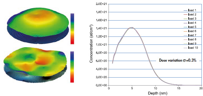
Repeatability test results of As dose measured in a 4keV As implanted wafer (10 loads/unloads).