The new Bruker Dimension IconIR is a large-sample nanoscale infrared spectroscopy and chemical imaging system. It sets new standards in chemical and material property mapping with sub-10nm chemical imaging resolution.
Join Bruker for a series of free online training sessions over the next few weeks, covering nanoscale surface analysis topic.

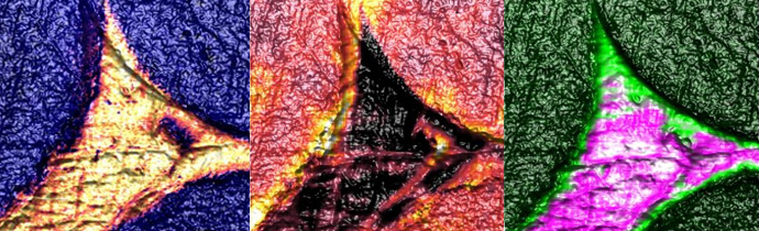
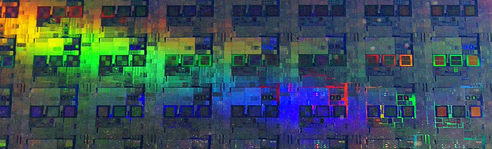
How nanoscale infrared spectroscopy can be used to measure semiconductor materials in defect and contamination analysis, and fabrication.
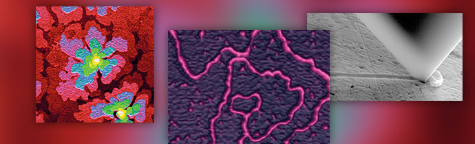
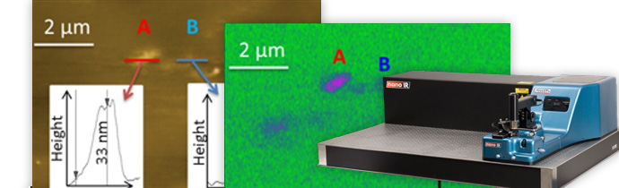
Unambiguously identify organic contamination on silicon wafers and micro-electronics with a AFM-IR technique, using the Bruker Anasys nanoIR3.
We’re now the official distributor for Bruker Anasys nanoscale infrared spectroscopy & thermal measurement instruments in the Nordic region (Denmark, Sweden, Finland, Iceland & Norway).

Bruker webinar about Peakforce SECM (Scanning Electrochemical Microscopy), a new AFM mode with less than 100 nanometre spacial resolution.
Come to our AFM workshop on Thursday 17th March 2016 at DFM (Danish National Metrology Institute) in Denmark.
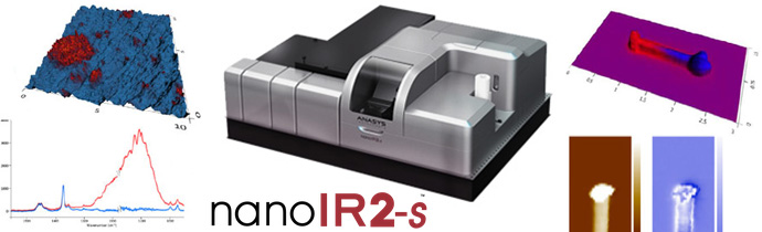
A new instrument from Anasys Instruments is the only nanoscale IR spectroscopy and imaging platform with both robust nanoscale IR absorption spectroscopy via AFM-IR and sub-20nm complex optical property imaging via sSNOM (scattering scanning near field optical microscopy). Follow Blue Scientific on Linked In for updates: UPDATE: This system has now been replaced with the Bruker Anasys […]
Diagnosing Surface Blooming of Polymer Additives Additives impart improved performance characteristics in polymer systems such as anti-oxidation, lubrication and UV protection. Surface blooming of additives can alter the bulk and surface properties of the material, leading to a range of undesirable outcomes from mechanical failure to cross contamination. For plastics in medical devices, changes of […]
AFM-IR can be used to study nanoscale protein secondary structure. This method provides valuable insights into biologically important macromolecules, which are not available using other analytical techniques. Blue Scientific is the exclusive distributor for Anasys AFM-IR instruments in the UK. If you have any questions or would like to see a demonstration, please get in touch: Contact us on 01223 […]