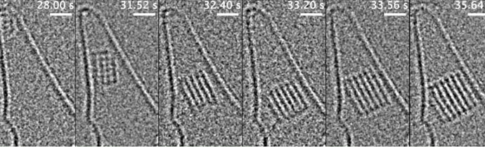
Capture dynamic processes during in-situ TEM experiments with the Gatan OneView IS camera, at up to 25 fps with 16 MP images. In this example, researchers at the University of Tokyo observed crystal nucleation and growth at atomic scale.

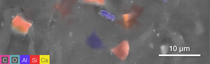
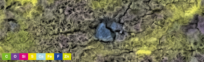
Combined SEM-EDS can be used to locate and identify contamination quickly and easily. The Thermo Scientific Axia ChemiSEM fully integrates the two techniques.
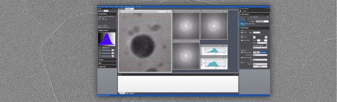
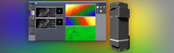
A series of video tutorials demonstrating how to use Gatan’s IS player, part of GMS 3 (Gatan Microscopy Suite) software for TEM/SEM.
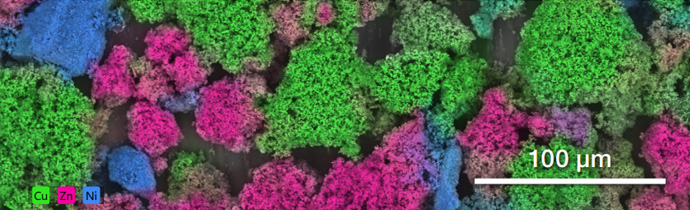
SEM-EDS can be used to characterise the composition of polymer composites. This is useful in failure analysis, to detect and identify contaminants and defects, and to check homogeneity.
Map defect distribution and variations for process development of materials for electronic / optoelectronic devices. CL is ideal for materials not suitable for photoluminescence spectroscopy.
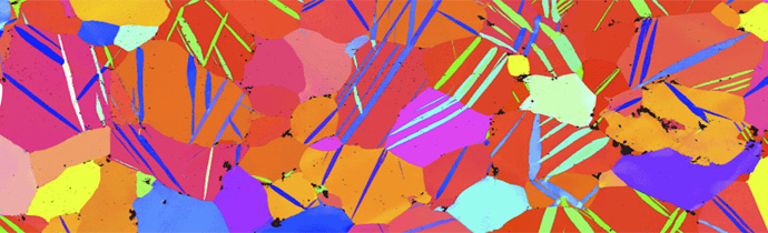
How SEM/EDS is used in failure analysis of steel, with examples of bend test failures, coating defects and corrosion in the automotive industry.
ColourSEM technology from Thermo Scientific combines SEM and EDS for easy-to-interpret elemental information, displayed live in colour on your SEM images. It’s fully integrated and always on, highlighting features on your sample that may otherwise be unnoticed. Blue Scientific is the official industrial distributor for the Thermo Scientific Axia ChemiSEM in the UK and Ireland. For […]
We’re proud to announce a new partnership with Thermo Fisher Scientific as official distributor of the Axia ChemiSEM scanning electron microscope in the UK and Ireland.
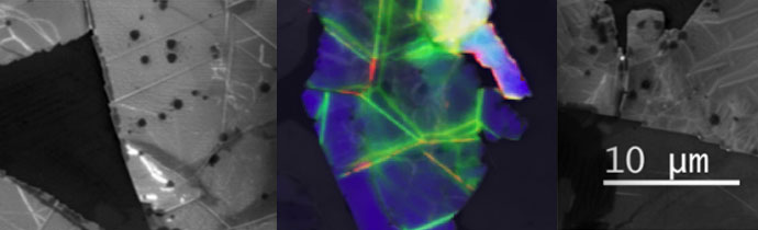
How to get better EBSD results by using ion milling to prepare samples, with the example of how to remove oxide layers from alloys