
Analyse Contaminants in Battery Materials with Combined SEM / EDS
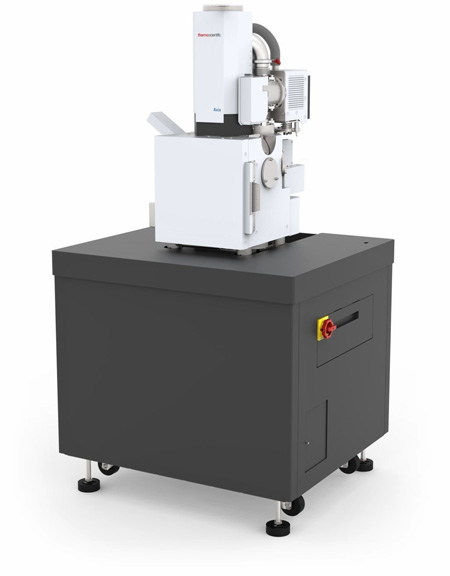
Contaminants in battery materials can cause issues with battery quality and performance. Combined SEM-EDS can be used to locate and identify contamination quickly and easily, providing information to help find its source. The Thermo Scientific Axia ChemiSEM fully integrates the two techniques. With point and click navigation and EDS data in colour, it’s easy to spot contamination, with fast results.
Blue Scientific is the official distributor for the Thermo Scientific Axis ChemiSEM in the UK and Ireland. For more information or quotes, please get in touch.
More about the Axia ChemiSEM
Contact us on +44 (0)1223 422 269 or info@blue-scientific.com
Contamination in Battery Materials
Contamination is a major issue at every stage of battery manufacturing, causing problems such as lower efficiency, cell degradation and even internal shorts.
Combined SEM and EDS can give you an understanding of contaminants that enter the battery manufacturing process. Using a Scanning Electron Microscope (SEM) and Energy Dispersive X-ray Spectroscopy (EDS), you can examine both the structure and elemental information of contaminants.
Traditionally, image acquisition times would be lengthy with conventional EDS for elements at such low concentration levels, making it a slow process. However, the new Thermo Scientific Axia ChemiSEM combines SEM and EDS in a single platform, making the process is much faster and simpler,and an extremely useful technique for micro-structural analysis of materials and defect discovery.
Investigate Contaminants in Battery Materials
With the Axia ChemiSEM, you can perform a thorough assessment of contaminants in battery materials, to improve battery quality and performance:
- Large-scale SEM-EDS mapping: Rapidly locate and identify contaminants.
- Detailed quantitative EDS analysis: Precisely pinpoint the distribution of each contaminant.
- Point analysis: Exact quantification of each element present in the contamination.
SEM imaging and EDS are no longer separate workflows – they’re fully integrated so you can progress from discovery to analysis and full results. It’s designed to make SEM easier to use, with automatic alignment and live “always on” EDS analysis.
Large-Scale Mapping
The Axia ChemiSEM has a large field of view so you can locate contaminants quickly. The view combines live quantitative elemental mapping and conventional SEM imaging. The example below is a low magnification image of a lithium cobalt oxide (LiCoO2) cathode, acquired for point and click navigation. It was collected within 15 minutes, including EDS data.
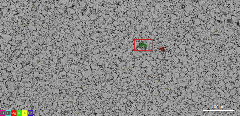
The image above includes elemental information, making it easy to locate foreign elements. From this initial navigation image you can then run a more detailed characterisation of the region of interest.
It’s extremely visual, and much easier and quicker to interpret than a standard greyscale backscattered electron image. Usually the compositional contrast between two different elements would be too similar to notice.
Detailed Analysis with SEM-EDS
Using the navigation image as a reference, you simply click on the point of interest to drive the stage to it.
Backscattered electron images from conventional SEM do not usually provide enough information to identify contaminants. However, the Axia ChemiSEM gives you virtually instant access to quantitative elemental information for every a greyscale image.
X-ray detection is always on; X-rays are acquired and processed in the background while the greyscale image is acquired. This provides quantitative elemental information, different from the raw signal usually acquired from a traditional EDS gross counts mapping analysis. Elemental information is constantly available, for a seamless characterisation experience and no time wasted waiting for data.
The quantitative elemental map below is of the area highlighted in the initial navigation image above. It was collected simultaneously during SEM image acquisition. This data can be viewed at any time by activating the quantitative elemental view. There’s no need to re-acquire data or wait for results like with conventional EDS.
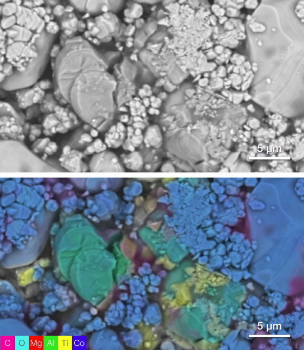
Bottom: Quantitative elemental mapping.
Acquisition time: 80 seconds.
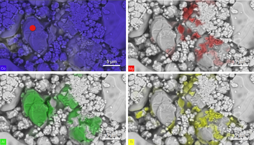
Highlight Single Elements
To visualise the distribution of each element, you can generate images highlighting single elements at a time, like the examples below.
In this example, Co is the main element in LiCoO2. However, Al, Mg, and Ti are also present in the electrode, which is unexpected. These contaminants may have been introduced during cathode materials synthesis, mixing or coating processes.
This enables you to locate elements that stand out, to discover contamination easily and identify possible sources.
Point Analysis
To further identify contaminants, point analysis can obtain the exact quantification of the elements present.
The data below is a point analysis of the red spot in the image above, giving full information about the contaminant at that spot.
This and the other functions mentioned in this article are fully integrated into the Axia ChemiSEM, using a single software interface and hardware system.
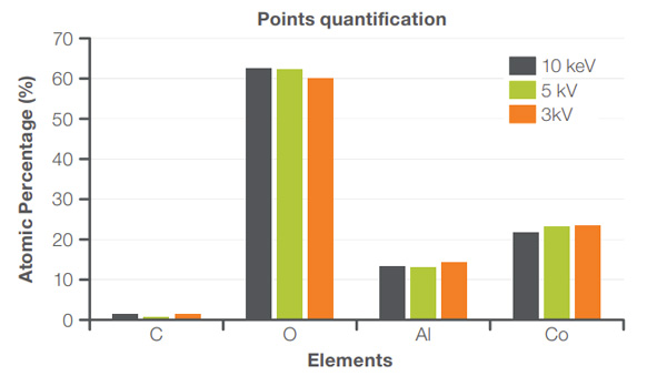
System alignment is automated, so analysis parameters can be changed without manual adjustment. This means you can easily perform point analyses at various accelerating voltages and beam currents.
In the data above, the composition remains consistent throughout the various conditions, showing that a certain amount of Al is embedded in the LiCoO2. This suggests that the Al element was reacting with the precursor used to synthesise LiCoO2 during sintering. This information can then be used to eliminate this source of contamination, by examining the raw materials for LiCoO2 synthesis or the sintering equipment.
Full details about these results are available in a pdf application note from Thermo Scientific.
Thermo Scientific Axia ChemiSEM
- Designed to make SEM more accessible and easier to use.
- Continuous EDS for quantitative elemental information at any time.
- Automated features for convenience.
- Acquire data twice as fast as alternative SEM-EDS systems.
- Large, flexible chamber.
More Information
Blue Scientific is the official distributor of the Thermo Scientific Axia ChemiSEM in the UK and Ireland. We’re available to provide quotes and answer all your questions – just get in touch: