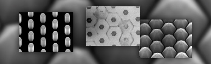
Studying Defect Formation in GaN Structures with AFM
Lund University in Sweden recently published two scientific papers about defects in GaN nanowires and structures, using AFM and various complementary techniques.
Blue Scientific is the official distributor for Bruker AFM in Norway, Sweden, Denmark, Finland and Iceland. For more information or quotes, please get in touch.
View the Bruker AFM range
Contact us on +44 (0)1223 422 269 or info@blue-scientific.com
Follow @blue_scientific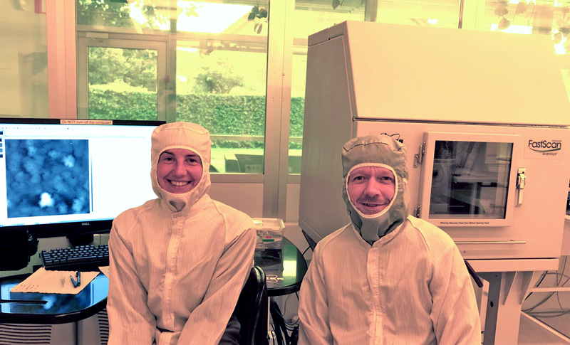
Defects in GaN Structures
The first paper from Lund University is entitled “Local defect-enhanced anodic oxidation of reformed GaN nanowires”. To improve the performance of rf and power electronics, it’s important to understand the formation and distribution of defects in GaN substrates and device layers.
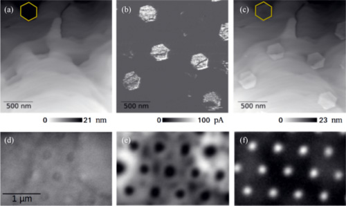
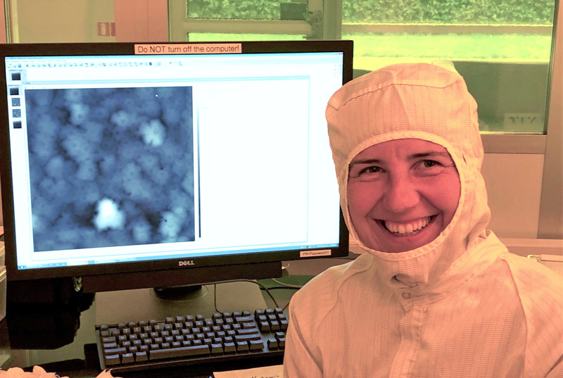
In this paper, researchers at Lund University used c-AFM (conductive atomic force microscopy) to investigate defect-related leakage paths in GaN film formed by nanowire reformation.
A nanoscopic Schottky contact was formed between the c-AFM probe and the GaN surface. Under reverse-bias conditions, this revealed local leakage currents around the nanowires. Cathodoluminescence revealed a high density of native and residual defects confined to the nanowires.
Anodic oxidation was used to map defect-related conductive paths through locally induced gallium oxide growth. The oxide yield depends on the local electric field strength between the AFM tip and the sample; this correlated well with the level of reverse-bias leakage current. Local irregularities in oxide height revealed extended oxidation related to defect-related deep-level states. This was confirmed by controlled dissolution of the oxide in NaOH, showing a deeper oxide film over defect-related conductive paths.
This approach could be used as a fast, easy diagnostic tool for evaluating the influence of specific growth conditions and process steps on defect-induced leakage current levels and defect distribution in GaN structures. This would be useful for rapidly testing leakage degradation at critical positions in GaN-based devices.
Read the full paper on APS Physics…
Higher Quality GaN Substrates from Nanowire Reformation
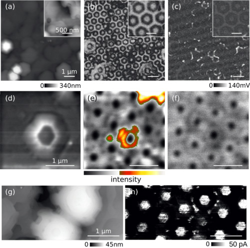
The second paper from Lund University is entitled “Surface and dislocation investigation of planar GaN formed by crystal reformation of nanowire arrays”. It presents a study of how to grow better quality GaN substrates through nanowire reformation.
The study involves forming a monolithic GaN surface from an ordered nanowire array using material redistribution, referred to as reformation. The crystal nanostructure changes shape in response to variations in surface energies between its facets. Thermodynamic equilibrium is required to create high quality substrate material.
Scanning probe techniques were used, together with cathodoluminescence and electron microscopy, to investigate structural and electrical properties of the surface after reformation. The density, location and formation of defects in the GaN film were also studied.
Spatial variations in material properties indicate changes in growth conditions for sequential transition between nanowire growth, selective shell growth and reformation. By measuring these properties, you can assess the impact of various processes on the density, location and formation of each type of dislocation in the GaN film.
The study reveals a method for improving crystal quality when growing GaN substrates using nanowire reformation.
Read the full paper on APS Physics…
Instrumentation
These instruments were used by Lund University in both of these studies:
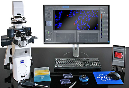
Bruker JPK NanoWizard 2
- Fast AFM imaging at 10 frames per second.
- Conductive AFM mode (optional).
- Correlative experiments with super-resolution, single molecule and advanced optical techniques.
Bruker Dimension Icon
- Versatile, large sample AFM.
- Widest range of AFM modes.
- Simultaneous electrical and property mapping at the nanoscale with PeakForce TUNA.
More Information
Blue Scientific is the official distributor of Bruker AFM in the Nordic region. If you’d like more information or advice on which system would complement your research, just get in touch: