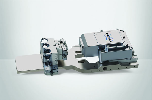
Hysitron PI 89 SEM PicoIndenter
NEW In-situ nanomechanical testing for SEM and FIB/SEM
The Bruker Hysitron PI 89 SEM PicoIndenter performs in-situ, quantitative nanomechanical testing while simultaneously imaging with your scanning electron microscopes (SEM, FIB/SEM).
The new system is the next generation of Bruker’s market-leading in-situ SEM nanomechanics platform. The PicoIndenter’s capabilities have been developed with extended force and displacement ranges, patented xR transducer technology and other exclusive advances.
The PI 89 is the most comprehensive in-situ nanomechanical test instrument for SEM and FIB/SEM available today, including:
- Electrical characterisation module
- Push-to-Pull (PTP) tension for thin films and nanowires
- Direct-pull tension
- Fatigue
- Rotation/tilt stage (patented)
- Testing at elevated temperatures
- Nanoscratch
Contact us for more information and quotes:
+44 (0)1223 422 269 or info@blue-scientific.com
Directly correlate mechanical data with microscope imaging, with real-time video capture from the SEM.
Features
- Extended range (10 mN, 500 mN, 3.5 N and 150 μm) in-situ nano- to micro-scale mechanical testing with Bruker’s proprietary interchangeable transducer technology.
- Exclusive load and displacement-controlled testing modes for nanoindentation, compression, tension, fatigue and bending tests.
- New encoded stage technology (1 nm resolution) for indentation within nanocrystalline grains.
- Two rotation/tilt stage configurations for improved sample positioning for nanomechanical testing, secondary electron imaging, in-situ FIB milling and analytical imaging.
- Modular design accommodates upgrades and testing techniques including:
- Heating up to 800°C
- Scratch testing
- Electrical characterisation
- SPM imaging (Scanning Probe Microscopy)
- Property mapping (XPM)
- Dynamic fatigue testing
- Capture transient events (eg fracture initiation) with a 78 kHz feedback rate and data acquisition up to 39 kHz, using Bruker’s Performech II Advanced Control Module.
True Displacement Control
The Hysitron PI 89 uses Bruker’s proprietary sub-nanometre sensitivity transducer and piezo-driven flexure for true displacement-controlled tests. Force is applied electrostatically by the low-load transducer, while simultaneously capacitively measuring displacement. Flexure-driven mode can be employed if you need a wider displacement range, up to a maximum of 150 μm.
The unique low-current design of the transducer minimises thermal drift and delivers unprecedented sensitivity. This is coupled to an encoded XYZ stage. The 12 x 26 mm range for sample positioning and 29 mm in indentation axis is useful for larger samples.
By integrating the sample stage and transducer on a single platform, it ensures a stable foundation for lateral precision, linearity and repeatability.
New Features for Convenience and Versatility
The Hysitron PI 89 mounts easily to the SEM stage. It can be removed and is not a permanent fixture. The instrument is compact, allowing for maximum stage tilt and minimum working distance for the best imaging results.
A new sliding stage mount enables you to adjust the sample position quickly and easily. It’s easier to swap probes, samples and add-ons, and leaves more space for larger samples, additional stages and new options.
New encoded linear stages increase repeatability during automated motions and extend the travel range. The mechanical load frame axis has also been redesigned to improved frame stiffness.
Testing Modes
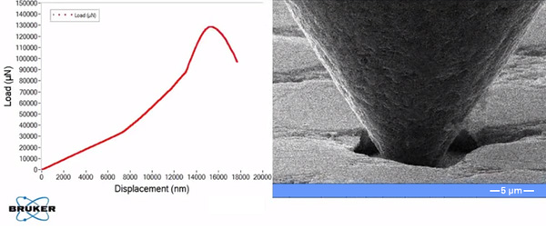
Nanoindentation
- Precise lateral positioning.
- Nanoscale load and depth control.
- Determine and quantify fundamental mechanical properties eg hardness, elastic modulus.
- Test a wide variety of materials.
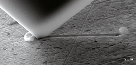
Tensile
- Direct-pull and push-to-pull (PTP) testing.
- Test dog-bone specimens, thin films and nanowires.
- Measure stress-strain behaviour in-situ in low dimensional materials that are difficult to test with standard methods.
Bending
- Accurate loading alignment and specimen size measurement using SEM imaging.
- Straightforward to measure bending stiffness and fracture toughness.
- Measure single-phase, composite and layered materials.
Compression
- Compress pillars, particles and other small scale structures.
- Measure stress-strain behaviour and yield properties.
- Simultaneously observe deformation mechanisms in real time.
- Tip alignment is verified using SEM imaging.
Optional Upgrades
- XPM high speed nanoindentation (500x faster) for nanomechanical property maps and distribution statistics.
- Heating up to 800°C.
- Electrical characterisation.
- nanoDynamic mode for viscoelastic and fatigue properties.
- Nanoscratch mode with simultaneous normal and lateral force sensing.
- Push-to-pull devices.