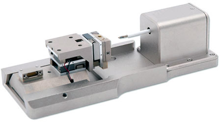
Bruker Hysitron PI 85L
Compact in-situ nanomechanical test system for SEM
The PI 85L SEM PicoIndenter is a depth-sensing nanomechanical test instrument for Scanning Electron Microscopes (SEM). Perform quantitative nanomechanical testing while simultaneously imaging with your SEM. Coupling these techniques also enables extremely accurate probe positioning.
- Nanoindentation, compression, tension and bending test modes
- In-situ data displayed beside SEM imaging for a complete picture of your sample’s behaviour
- Compact design for small chamber SEMs, Raman, beamlines and optical microscopes
- Optional upgrades for extra capabilities, including heating and electrical characterisation
Contact us for more information and quotes:
+44 (0)1223 422 269 or info@blue-scientific.com
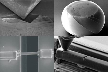
Testing Modes
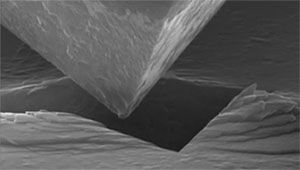
Nanoindentation
- Precise positioning
- Nanoscale load and depth control
- Determine fundamental mechanical properties eg hardness and elastic modulus
- Suitable for a wide variety of materials
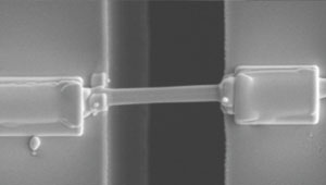
Tensile
- Direct-Pull and Push-to-Pull (PTP) testing
- Test dog-bone specimens, thin films and nanowires
- Measure stress-strain behaviour in-situ
- Study low dimensional materials not easily tested with traditional methods.
Bending
- Align loads and measure accurately with SEM imaging
- Measure bending stiffness and fracture toughness
- Single-phase, composite or layered materials.
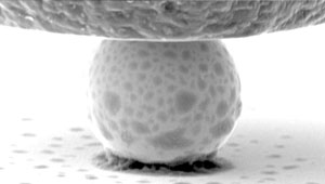
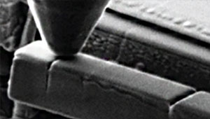
Compression
- Compress pillars, particles and other small scale structures
- Measure stress-strain behaviour and yield properties
- Simultaneously observe deformation mechanisms in real time
- Check tip alignment with SEM imaging
Optional Upgrade Modes
- Heating up to 800°C
- Electrical characterisation
- Push-to-pull device
- nanDynamic mode
- nanoScratch mode
Technical Details
The PI 85L SEM PicoIndenter is the latest generation of Hysitron’s in-situ nanomechanical testing system. It was originally designed for SEM but the low profile is also suitable for Raman, optical microscopes, beamlines and more.
- Extremely fast 78kHz control system
- Accommodates samples up to 10 mm thick
- Precise sample positioning with >3 mm in all three directions (XYZ)
- Mechanically coupled sample stage and transducer for rigid stability
- Designed for maximum stage tilt and minimum working distance, for the best imaging set-up
- Active vibration dampening, with proprietary Q-Control technology
- Transducer technology with electrostatic actuation and capacitive displacement sensing
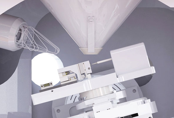
Hysitron PI85L inside an SEM chamber