Up to 100mm x 100mm
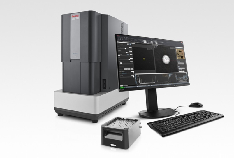
The Thermo Scientific Phenom ParticleX AM is a desktop SEM (Scanning Electron Microscope) for additive manufacturing analysis, for large samples up to 100 mm x 100 mm.
Up to 100mm x 100mm
Fast to learn
A growing number of manufacturing companies are using SEM analysis in-house instead of outsourcing. This equips you with a range of automated analyses, chemical classification and verification according to specified norms.
The Thermo Phenom ParticleX is fast, to support production with accurate verification and classification of materials. It’s automated and can analyse multiple samples for high throughput.
Outsourcing can take up to 10 working days, whereas with the Phenom ParticleX results are ready within a day. It’s simple to operate, fast to learn and doesn’t take up too much space as a desktop instrument.
The Phenom ParticleX can also take on tasks from other SEMs in the lab – for example particle analysis of metal powders at the microscale for the additive industry, and confirming that components fulfill technical cleanliness specifications (according to VDA19 or ISO16232 standards).
Thermo’s proprietary venting/loading mechanism gives you the world’s fastest vent/load cycle, with an industry-leading sample-loading time of 60 seconds or less. This provides higher throughput than other SEM systems.
Measure various size and shape parameters with 10%, 50%, 90% values (e.g. d10, d50, d90):
It’s easy to perform line scans and elemental mapping: simply click and go! Element mapping visualises the distribution of elements. Line scans show the quantified element distribution in a line plot – particularly useful for coatings, paints and applications with multiple layers, for analysing edges, coatings, cross sections, etc. Reports can then be exported easily using templates.
An optional secondary electron detector is available for the Phenom ParticleX AM. This collects low-energy electrons from the top surface layer, for detailed information about the surface. This is useful in applications where topography and morphology are important eg microstructures, fibres or particles.
The Thermo Scientific Phenom ParticleX AM is perfect for the routine inspection of materials, when the identification and reporting of particle sizes, shapes, and elemental chemistry are critical to manufacturing operations.
Additive manufacturing requires feedstocks to be examined carefully, particularly when recycled powders are used, to ensure the integrity of printed materials and to maintain batch-to-batch consistency.
A recorded webinar from Thermo Scientific about how to match the features and specification of a SEM to the requirements of your application.